
Course Description
Virtually every electronic product is constructed with one or more printed-circuit boards (PCBs). The PCBs hold the ICs and other components and implement the interconnections between them. The ideal PCB design starts with the discovery that a PCB is needed and continues through the final production boards.
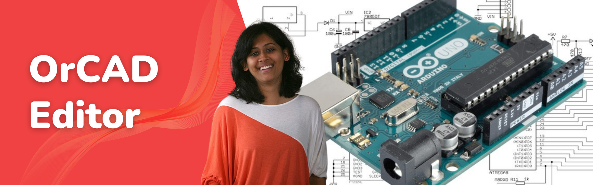
OrCAD PCB Editor contains full-featured PCB editor based on Allegro technology. Its extensive feature set addresses a wide range of today’s design challenges and manufacturability concerns such as intelligent placement and routing, constraint management, creating dynamic shapes, and design reuse.
JOB OPPORTUNITIES
some of the jobs available for students at electronic and hardware manufacturing companies are
- PCB Designer, Design Engineer – PCB,
- Technical Lead – PCB Layout,
- Design Engineer – Electronics,
- Project Leader – Electronics,
- Hardware Engineer,
- Lead Engineer – Motor Design.
As India is developing in Electronics field tremendously, there is huge demand in this field.
The average pay for an Electronics Design Engineer is Rs 400,431 per year.
WHO CAN ENROLL?
Students pursuing their Bachelors, Diploma or Masters in ECE, EEE, E&I and industry professionals.
-
WHAT WILL I LEARN?
- Schematic Modification for PCB Design
- Design Rule Check
- Pad Designer
- Package Symbol & Package symbol wizard
- Netlist creation
- Component and board placement
- Mechanical symbol placement
- Manual and Automatic routing
- Constraint Manager and Xsection
- Blind, Buried and through-hole VIA
- Copper shaping
- Artwork/Gerber file creation
- Plot Generation
- PCB Fabrication Process